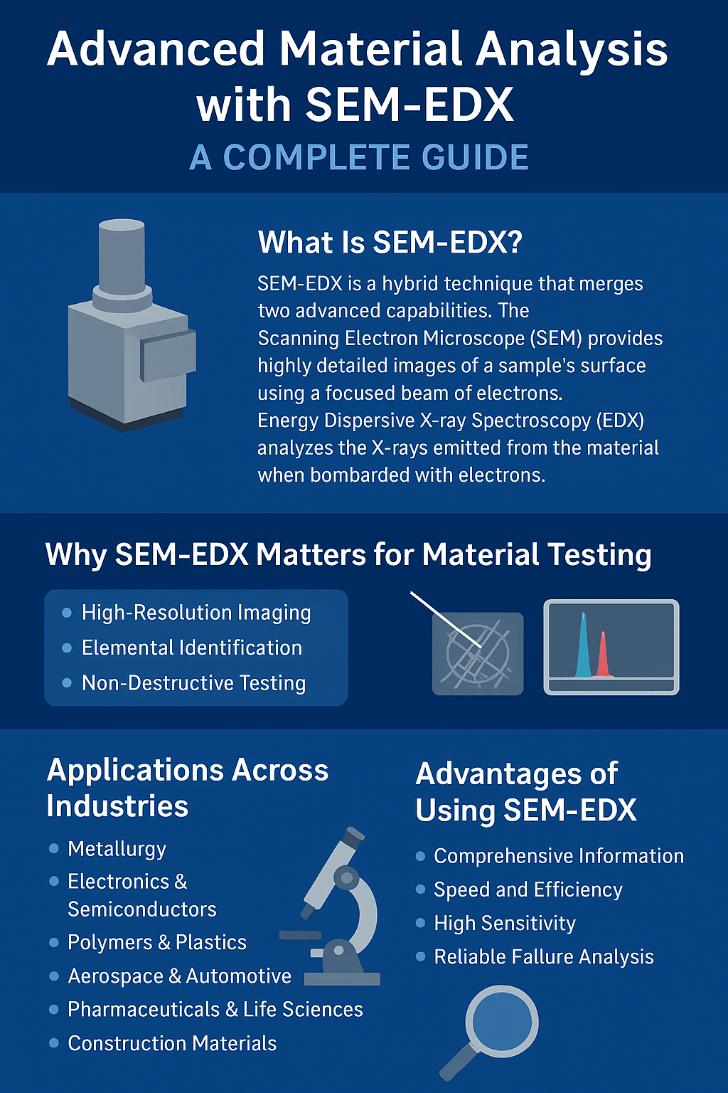
In today’s fast-evolving industrial and research environment, understanding the microscopic structure and elemental composition of materials is essential for improving quality, performance, and reliability. One of the most trusted analytical techniques used across laboratories and industries is SEM-EDX (Scanning Electron Microscopy with Energy Dispersive X-ray Spectroscopy). This powerful combination allows experts to study materials at extremely high magnifications while simultaneously identifying the elements present in them. Whether in manufacturing, metallurgy, electronics, or academic research, SEM-EDX has become an indispensable tool for precise material characterization.

What Is SEM-EDX?
SEM-EDX is a hybrid technique that merges two advanced capabilities. The Scanning Electron Microscope (SEM) provides highly detailed images of a sample’s surface using a focused beam of electrons. This level of magnification reveals minute features such as cracks, grain structures, surface textures, and defects that are impossible to detect with conventional microscopes.
Alongside this, Energy Dispersive X-ray Spectroscopy (EDX) analyzes the X-rays emitted from the material when bombarded with electrons. These X-rays carry information about the sample’s chemical composition. By capturing and interpreting these signals, EDX identifies the elements present and their relative proportions. This dual approach gives both visual and compositional insights in a single analysis.
Why SEM-EDX Matters for Material Testing
Material testing demands both structural and elemental accuracy. SEM-EDX delivers on both fronts, making it widely applicable across industries:
1. High-Resolution Imaging
SEM images provide unmatched clarity, enabling professionals to detect micro-cracks, corrosion patterns, fractures, and material inconsistencies. This is crucial for failure analysis, product development, and quality evaluation.
2. Elemental Identification
With EDX, users can pinpoint which elements are present in even the smallest region of a sample. This is especially useful in metallurgy, electronics, polymer analysis, coatings, and contamination studies.
3. Non-Destructive Testing
SEM-EDX does not require major sample alteration. This makes it suitable for analyzing delicate materials, electronics components, and forensic samples without compromising integrity.
4. Micro-Area Analysis
The technique allows targeted testing of specific micro-zones, which is essential when studying layered materials, inclusions, or localized defects.
Applications Across Industries
SEM-EDX is used in a wide range of sectors due to its unmatched capabilities:
Metallurgy: Identifying inclusions, corrosion, grain boundaries, and alloy structures.
Electronics & Semiconductors: Studying component failures, solder joint quality, and contamination.
Polymers & Plastics: Understanding filler distribution, surface defects, and degradation.
Aerospace & Automotive: Analyzing fatigue failures, coatings, and wear patterns.
Pharmaceuticals & Life Sciences: Examining particulate matter, coatings, and morphology.
Construction Materials: Investigating concrete failures, aggregates, and surface roughness.
The versatility of SEM-EDX makes it a first choice for anyone needing detailed and dependable material characterization.
Advantages of Using SEM-EDX
Comprehensive Information
Few techniques offer both imaging and elemental data in one platform. This holistic view accelerates troubleshooting and ensures more accurate interpretations.
Speed and Efficiency
SEM-EDX delivers results quickly, making it ideal for industries that require fast decision-making, such as electronics manufacturing and process control.
High Sensitivity
Even trace elements can be detected with strong accuracy, supporting detailed research and quality assessments.
Reliable Failure Analysis
By revealing root causes at the micro-level, SEM-EDX helps prevent repeated failures and enhances product safety and performance.
Conclusion
SEM-EDX stands out as one of the most valuable tools in modern material analysis, offering unmatched detail and precision. By combining powerful electron imaging with accurate elemental identification, it supports industries in improving quality, solving failures, and advancing research. For any organization aiming to achieve higher reliability and deeper insights into material behavior, SEM-EDX remains a vital technology.


Write a comment ...